
Scanning Electron Microscopy

The working principle of a scanning electron microscope (SEM) is to prepare an extremely fine electron probe and let it interact with the sample surface. Upon the interaction of the (primary) electrons with the sample material, different electrons escape from the examined surface and are detected with a variety of detectors. Depending on their energy, the emanating electrons were classified as secondary electrons (SE) and backscattered electrons (BSE).
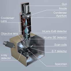
The principal components of any SEM are the electron gun with the anode, the condenser system, the objective lens, the scan coils and the detection system.
Electron emitter (Gun)
As obvious from the name, the electron emitter or electron gun has the purpose to provide the electrons which are then guided through the column. In commercially SEMs three different types of electron guns are used: tungsten filament, LaB6 cathode or field emission guns (FEG). The latter has the highest luminosity and provides high beam currents. However, tungsten filaments and LaB6 cathodes are still in operation in many SEMs due to their low cost compared to a FEG and these emitters still do a very good job.
Once the electrons have been generated by the electron gun, they have to be accelerated in order to traverse the column down to the specimen. This is done by placing an anode close to the emitter. The anode is set to a certain positive potential which can be adjusted from 0.1 to 30 kV. After passing the hole in the anode, the electrons enter the condenser system of the SEM.
Condenser system
The condenser system of a SEM is usually composed of several electromagnetic lenses and apertures. It´s purpose is to provide a convergent electron beam. After leaving the condenser system the electron beam enters the objective lens.
The objective lens
focusses the electron beam further to achieve a very fine electron spot on the sample surface. In modern SEMs the objective lens is composed of electrostatic- and electromagnetic lenses and a highly sensitive pole-piece. It is the operators highest concern to avoid any pole-touch with the sample.
The scan-coils
are incorporated into the lower part of the objective lens system / pole-piece. They deflect the electron beam in x- and y- direction in order to scan the sample surface. The information is then recorded by the
Detector system
which actually yields a current signal from the respective beam position. Together with the position of the electron probe on the sample and the corresponding detector signal the SEM produces some kind of “image” of the sample. But one must keep in mind that this image is nothing else than the visualization of the local SE / BSE emission intensity. It´s not a real image.
However, the modern SEM detector design is quite sophisticated and many different detectors yield a lot of different information on the local composition of the sample. Especially the InLens detector systems, where the electron detectors are located “upstream” in the column yield superior information and produce superb micrographs.
Scanning electron microscopes at the MPI-P
At the MPI-P we operate two SEMs. These SEMs are equipped to serve all the demands of the scientists in the MPI-P. For our students the LEO Gemini 1530 is the perfect SEM to collect first experience in scanning electron microscopy and to “see” their own samples. It´s superb imaging properties and easy handling, especially at low kV conditions, made it the working horse to observe nearly any samples prepared at the MPI-P.
To facilitate more demanding examination problems, the EM-group operates a Hitachi SU8000 equipped with energy dispersive x-ray detector and cryo-preparation device.